Many consider MicroLED technology to be the next disrupter in the display market. The performance of MicroLEDs, which are small light-emitting diodes, is significantly better than those of conventional LCD and OLED screens.
The technology involving MicroLED extends beyond just high-quality displays. It gives higher brightness, better color accuracy, quicker response times, and lower power consumption. These benefits make MicroLED production beneficial for diverse sectors, including consumer electronics, automotive, and more.
However, the path to mass manufacturing of MicroLEDs is fraught with challenges.
A 4K MicroLED display has over 24 million subpixels, and even at very high yields, defective LEDs cannot be avoided. Moreover, the MicroLED market is expected to expand to $1.46 billion by 2028.
This article will look into these challenges, with a particular focus on the patents that are paving the way for overcoming these hurdles and realizing the full potential of MicroLED technology.
Understanding MicroLED Technology for MicroLED Production
MicroLED is a newer display technology that uses millions of small microscopic light sources. Each pixel emits its own light independently, resulting in similar display characteristics to OLED.
However, the technology doesn’t rely on organic materials, making it far more durable and capable of reaching higher brightness levels without the fear of degradation.
The MicroLED market size is expected to grow from USD 1.06 billion in 2023 to USD 21.29 billion by 2028, at a CAGR of 82.19% during the forecast period (2023-2028).
This growth is primarily driven by its adoption in wearable devices like smartwatches, AR glasses, and automotive displays.
Challenges in MicroLED Production
The key challenges hindering the mass manufacturing of MicroLEDs are:
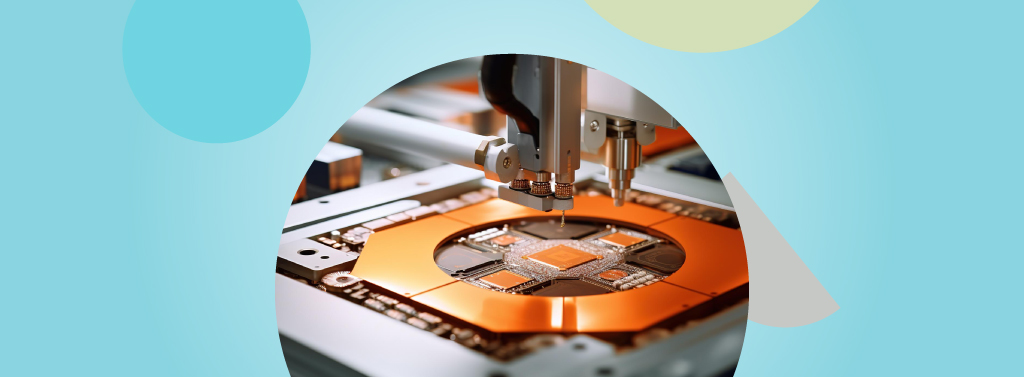
- Complex Manufacturing Process: MicroLED production involves a multi-phase process that includes epitaxial growth, photolithography, chip fabrication/wafer fabrication, substrate removal, mass transfer, bonding and interconnection with the control circuit, testing, repair, panel assembly, etc. The complexity of this process contributes to the challenges in MicroLED production.
- Issues Related to the Size of MicroLEDs: MicroLEDs are close to the size of a neuron, which could have an impact on how some illnesses are monitored and treated. Due to their tiny size, a key production bottleneck for displays made with MicroLEDs is the “mass transfer” of MicroLED-bearing chips from the wafer to the display backplane. These transfers involve millions of MicroLEDs and must be executed with microscopic accuracy.
- Problems in Mass Transfer Process: The mass transfer process of MicroLEDs is a significant challenge. There are many challenges in the MicroLED mass transfer process, including equipment accuracy, transfer yield, time of mass transfer process, manufacturing technology, inspection method, rework, and processing cost. A patent application titled “Laser Projection Proximity Mass Transfer Device, Method, and Equipment” discloses a projection proximity mass transfer device that includes a support layer, a dynamic release layer, and an adhesive foam layer.
- High Cost Associated with MicroLED Technology: MicroLED displays continue to be expensive, which inhibits adoption for everyday personal devices. They are expensive because it’s technologically challenging to arrange them into a display. As of the first quarter of 2021, more than $5 billion has already been spent on MicroLED development.
Patents in MicroLED Production
The number of MicroLED patents is now over 8,900, filed by almost 480 organizations. 40% of the patent families were published in 2020.
LG Display acquired 14 MicroLED-related patents from Taiwan-based Ultra Display Technology.
The patents mostly detail MicroLED transfer technology, but some are also related to MicroLED microdisplays.
Here are some companies that have been actively filing patents in the MicroLED technology space:
- AvicenaTech Corp.: Based in California, United States, AvicenaTech Corp. is a startup that has filed 19 patents related to MicroLED technology. One of their patent, titled “Coupling Microleds to Optical Communication Channels,” describes a method where light from one or more MicroLEDs may be coupled into multiple waveguide cores. This is significant for optical communication systems.
- Prilit Optronics, Inc.: This company is based in Taiwan and has filed 17 patents. One of their patent titled “MicroLED display panel” describes a microLED display panel that includes microLEDs, a substrate for supporting the microLEDs, and a plurality of chip-on-film (COF) packages mounted on surfaces of the sub-regions respectively, with a plurality of drivers being disposed on the COF packages.
- Intel Corp.: Intel Corp., a well-known multinational corporation and technology company headquartered in California, United States, has filed 17 patents. Intel has a total of 214,150 patents globally, out of which 123,905 have been granted, and more than 48% of these worldwide patents are active. It has filed the maximum number of patents in the US, followed by Germany and China.
- eLux, Inc.: eLux, Inc. is a startup based in Washington, United States, that has filed 9 patents. The company has been awarded a US patent of 9,825,202 titled “Display with Surface Mount Emissive Elements” for a microLED display based on assembly using massively parallel fluidic assembly. They also claim that it can assemble 50 million microLEDs per hour.
- Nanosys, Inc.: Based in California, United States, Nanosys, Inc. has filed 6 patents. Nanosys has secured over $50 Million in growth capital financing for the expansion of quantum dots for LCDs and accelerates the commercialization of microLED and nanoLED display technologies.
- Corning, Inc.: Corning, Inc., a company based in New York, United States, known for its expertise in glass, ceramics, and related materials science, has filed 5 patents. Corning has developed a process to create wrap-around electrodes (WAEs) on glass for use in tiled microLED display applications. The electrodes have small size and spacing, low resistance, and good reliability.
- Raxium, Inc.: Raxium, Inc. is a startup based in California, United States, that has filed 4 patents. Raxium has filed for patents to protect various inventions. One of them is the “Partial light field display architecture,” which forms microLEDs that exhibit high current density operation and long operational lifetime.
- Point Engineering Co., Ltd.: Point Engineering Co. Ltd, based in Chungcheongnam-do, South Korea, has filed 3 patents. Point Engineering Co., Ltd. has a patent titled “Inspection method for micro LED,” which is configured to inspect whether the micro LED is defective.
End Note
The transformative potential of MicroLED production in the display market is undeniable, offering superior performance and advancements in various sectors. Despite challenges in mass manufacturing, ongoing research and a surge in patent filings reflect a collective effort to address complexities in the process, size-related issues, mass transfer problems, and high costs associated with MicroLEDs.
Key industry players, including AvicenaTech Corp., Prilit Optronics, Inc., Intel Corp., eLux, Inc., Nanosys, Inc., Corning, Inc., Raxium, Inc., and Point Engineering Co., Ltd., contribute innovative solutions through active patent filings. With over 8,900 patents from nearly 480 organizations, collaboration is essential for future breakthroughs.
The future of MicroLED production lies in continued research, collaboration, and knowledge-sharing, ensuring the technology realizes its full potential across diverse applications. Join the community shaping the next era of display technology.
For updated information on this topic, take a look at our resources with frequently-updated information.