MicroLED display, utilizing tiny self-emissive LED pixels, offer superior optical and electrical properties compared to traditional LCD and OLED technologies. With enhanced brightness, energy efficiency, and wide viewing angles, microLEDs are poised to revolutionize displays for augmented/virtual reality, wearables, and future Apple products.
As per Straits Research report, the global microLED display market is set to boom. By 2031, projections indicate it will reach a remarkable USD 19,250 million, with a CAGR of 88%.
Despite such potential, guaranteeing high-quality manufacturing remains a constant pain point. It also stunts production efficiency. On top of that, uniformity Issues and quality challenges must be addressed before commercially viable microLED display solutions are available.
Let’s dive into the specific challenges and solutions for microLED display inspection and quality control.
Uniformity Issues and Solutions in MicroLED Display
MicroLEDs produce high brightness and color variations and are easily perceptible to the human eye. However, their visual performance falls short of display requirements, with slight color reproduction variations due to semiconductor characteristics or fabrication processes. Here are some major uniformity issues and their solutions:
1. Global and Local Dimming
Display manufacturers can utilize global dimming techniques to adjust the display’s brightness to account for brightness variations.
Global dimming techniques enhance image quality in dark scenes in movies or games by reducing display brightness, while bright scenes can be brightened to maintain optimal visibility and contrast.
This involves adjusting the brightness of LEDs by varying electrical current. Furthermore, local dimming may dynamically adjust the brightness of certain panel sections, ensuring consistent lighting.
2. Color Calibration
Some decent color calibration algorithms can match the color output of each MicroLED and compensate for differences in color reproduction.
For instance, Samsung has introduced self-calibration technology for its MicroLED displays, utilizing built-in sensors and algorithms to monitor and adjust the color output of each pixel in real time, ensuring consistent color reproduction across the entire screen. By calibrating each MicroLED independently, display makers can reduce color variations.
3. MicroLED Uniformity Control
Advanced manufacturing procedures can help increase the uniformity of MicroLEDs, which includes optimizing fabrication procedures to ensure each MicroLED has a consistent size, shape, and intensity.
In recent years, colloidal quantum dots (QDs) have emerged as a viable emissive material for substituting organic or molecular phosphors in phosphor-converted LEDs.
For instance, Samsung uses quantum dot technology in QLED displays, replacing traditional phosphors with blue LEDs. Quantum dots convert blue light into red and green, resulting in a wider color gamut and higher color accuracy.
These QDs are nanoscale semiconductor crystals that display characteristics unique from bulk semiconductors.
Furthermore, integrating MicroLEDs with quantum dots rather than passive color filters can widen the display’s color spectrum.
4. Demura Method
One advanced technique to address microLED display uniformity issues is the Demura method. This involves rigorously testing and calibrating each individual subpixel on the display to correct for brightness and color output variations.
The key steps are as follows:
- Test individual subpixels on the display with distinct color sets using a high-resolution imaging colorimeter to determine the brightness values at each pixel coordinate point.
- Test images are projected onto target subpixels of each color to measure and calculate the correction factors for each set. For example, green test photos show green subpixels that the imaging colorimeter measures and records.
- Red, green, blue, and frequently white are the primary colors for which this process is repeated. A coefficient calculator is filled with the measurement data obtained from the coordinate point of each display pixel.
- Afterward, the correction factors are calculated to correct for differences in chromaticity and brightness between pixels to measure and calculate the correction factors for each set.
- Finally, use a to apply these correction factors to each subpixel’s signal at each pixel location.
Defect Management Challenges in MicroLED Display Production
A rigorous approach is required throughout manufacturing to produce high-quality MicroLED displays. To begin, selecting a low-defect method at each level is critical. Subsequently, choosing epitaxial growth equipment and techniques requires a balance between minimizing flaws and maximizing efficiency. Also, prioritizing fewer flaws may be necessary, even if it increases costs.
1. MicroLED Wafer Fabrication
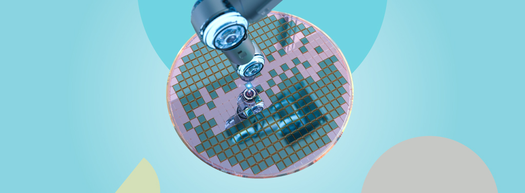
New inspection methods are crucial, as standard probing is impractical for microLEDs’ tiny size. High-speed, non-destructive optical techniques like micro-Raman and photoluminescence could enable in-line monitoring during epitaxial growth, lithography, and etching.
Achieving high uniformity across the wafer in terms of microLED dimensions, wavelength, and intensity remains a key challenge.
2. Handling Flaws in Final Product
The display panel remains challenging in handling flaws in the finished product. Potential methods include repairing faulty pixels with repeat transfers or implementing redundancy by doubling the number of MicroLEDs in each subpixel.
However, establishing efficient defect management technologies for the panel remains a problem. Therefore, a comprehensive approach that includes all production processes is required, with each enhancement possibly easing the following steps.
For example, increasing epitaxial growth uniformity can reduce the requirement for extra sorting based on wavelength and brightness. By systematically solving these obstacles, the objective of making faultless MicroLED displays becomes more achievable.
Techniques for Improving MicroLED Efficiency
Researchers have developed a number of methods to improve microLED efficiency:
Size-Dependent Efficiency Trends
UCSB research states that green MicroLEDs have a lesser efficiency decline with decreasing size than blue MicroLEDs smaller than 10 µm. This results in better External Quantum Efficiencies (EQEs) despite lower green efficiencies in larger-area LEDs.
Benefits of InGaN Red MicroLEDs
Furthermore, using InGaN red LEDs has further benefits because all RGB microLED devices are based on III-nitride with uniform properties and driving configurations, simplifying fabrication, transfer, and backplane technologies.
Addressing Sidewall Defects
The main issue requiring improvement in microLED performance is non-radiation recombination caused by sidewall defects from dry etching plasma-induced damage. Techniques like mesa etching, annealing, passivation, and wet etching have been developed to improve microLED EQE by minimizing sidewall defects.
As a result, certain research groups are concentrating on developing InGaN RGB microLED displays, exploiting these advantages to improve performance and production efficiency.
Microlens for Extraction Efficiency
The microlens are proposed for extraction efficiency and control of the emission direction of the microLED.
To Sum It Up
MicroLED Display has many advantages compared with current LCD and OLED displays, leading to a wide range of applications and huge markets. At the same time, the tiny chip size and high requirements for display applications cause many problems and strict specifications in each manufacturing step.
From epitaxial wafer growth to panel manufacturing, the extended supply chain also causes problems in system design and complex processes.