Introduction
Conventional displays, such as OLED and LCD, have limits with respect to brightness, scalability, durability, and image quality. This can be a problem for users who desire an exceptional viewing experience, large-scale displays, or curved screens.
MicroLEDs address these limitations by offering superior image quality, unmatched brightness and color vibrancy, modular design for scalability, and improved durability.
A recent study estimates that the microLED industry will grow from $0.74 billion in 2024 to $1.48 billion in 2029.
This corresponds to an amazing annual growth rate of 81.8%.
So, microLEDs will likely be a dominant display technology of the future since they deliver higher display quality at lower power consumption. This blog post will provide a thorough understanding and an in-depth analysis of the microLED fabrication process.
Understanding the MicroLED Fabrication Process
MicroLEDs, the building blocks of cutting-edge microLED displays, are made of inorganic materials like gallium nitride (GaN), a common component in standard LEDs. This composition gives them superior brightness compared to OLED and LCD displays, making them exceptionally visible even in direct sunlight.
MicroLED Fabrication Process: An Outline
The microLED fabrication process is intricate, involving multiple stages:
- Epitaxial Growth: The creation of the initial microLED wafer.
- Photolithography: Patterning the wafer using light-sensitive materials.
- Chip/Wafer Fabrication: Forming individual microLED chips.
- Substrate Removal: Separating the microLEDs from the original wafer.
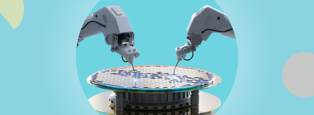
- Mass Transfer: Precisely positioning thousands of microLEDs onto a display backplane.
- Bonding and Interconnection: Connecting the microLEDs to control circuitry.
- Testing and Repair: Ensuring optimal display quality.
- Panel Assembly: The final integration of components into a complete display.
Patent Landscape of MicroLED Technology
According to French market research firm Yole Développement,
As of the end of last year, nearly 5,500 patents in µLED technology had been filed by more than 350 different organizations, with some 40% of the patent applications coming in 2019 alone.
Now, let’s explore some key patents related to the microLED fabrication process.
1. US10297712B2 – MicroLED display
Apple Inc. holds a patent that outlines the design and formation of a micro light-emitting diode (LED) and the method for forming an array of these microLEDs. This array is designed to be transferred to a receiving substrate.
Key aspects of the patent include:
- The microLED structure may comprise a micro p-n diode and a metallization layer.
- The metallization layer is positioned between the micro p-n diode and a bonding layer.
- A conformal dielectric barrier layer could span the sidewalls of the micro p-n diode.
- The microLED structure and the microLED array can be picked up and transferred to a receiving substrate.
2. US10636349B2 – MicroLED display device and method of fabricating the same
This patent reveals a microLED display device that can produce high-resolution full-color images. The key components of the device are:
- A microLED driving substrate where numerous CMOS cells are organized in a grid pattern.
- A microLED panel that is flip-chip bonded onto the microLED driving substrate. This panel contains several microLED pixels that are electrically connected to the CMOS cells.
It has numerous microLED pixels created by etching the first surface of an emission structure along a unit pixel region.
Additionally, several separators are on the second surface of the emission structure. These separators correspond to the positions of the sections formed by vertically etching the emission structure.
MicroLED Fabrication Process: Key Players in the Field
These companies have been accelerating their microLED development efforts and have a strong presence in the patent landscape.
- Apple (US): Apple is a technology giant that is heavily invested in the development of microLED technology.
- Oculus VR (US): Known for its virtual reality hardware, Oculus is also making strides in microLED development.
- Sony (Japan): Sony is not only a major player in the microLED field, but it also sells microLED displays as a replacement for conventional cinema screens.
Several other leading companies are at the forefront of microLED technology. For example, LG, Tianma, PlayNitride, TCL / CSoT, Jasper Display, Jade Bird Display, X-Celeprint (Ireland), Samsung Electronics (South Korea), Plessey Semiconductors Ltd, and Ostendo Technologies, Inc. have demonstrated prototypes.
Other organizations like Seoul Semiconductor and Konka Group are also leading the industry’s innovation efforts.
Recent Developments in MicroLED Fabrication Process
The microLED fabrication process has seen significant advancements in recent years. Here are some key developments:
Chip Technology
The challenge lies in improving the uniformity of wavelength and current density in microLED chips, which is crucial for achieving high-quality displays.
Research is ongoing with methods like incorporating transparent conductive layers or distributed Bragg reflectors within the microLED structure to achieve uniform current density and improve overall light extraction efficiency.
Mass Transfer
This is the process of transferring microLEDs from an epitaxy wafer to a substrate. The efficiency and yield of this process have been the focus of recent research, some of which are:
- Laser-induced Transfer (LIT): This technique utilizes focused laser pulses to detach microLEDs from the growth substrate and precisely transfer them onto the target display backplane.
Advancements focus on optimizing laser parameters and transfer conditions to minimize thermal damage and improve transfer yield (percentage of successfully transferred microLEDs).
- Roll-to-Roll Transfer: This approach aims to transfer microLEDs continuously from a flexible growth substrate to a roll-based display backplane.
Research is directed towards developing robust and scalable roll-to-roll processes with high throughput and minimal defects.
Bonding and Driving Technology
Research is being conducted to simplify this process and develop more efficient integration methods.
- Backplane Integration with TFT Arrays: Integrating Thin-Film Transistor (TFT) arrays directly onto the backplane substrate eliminates the need for a separate transfer process for driver circuits. This research focuses on miniaturization and high-density integration of TFTs to achieve high-resolution displays.
- MicroLED Array Backplane with Microgated Emitters: This approach involves fabricating microelectrodes directly on the backplane substrate, enabling individual microLED control without a separate TFT array. Research explores optimizing micro-electrode design and fabrication processes for efficiently addressing and driving microLEDs.
Chip Detection and Repair Technologies
These technologies are crucial for identifying and fixing faulty display pixels during the fabrication process. This can help ensure near-perfect visual quality in the final product.
- Automated Optical Inspection (AOI): Implementing advanced machine vision systems equipped with high-resolution cameras and image processing algorithms allows for automated detection of microLED defects during the transfer and bonding process.
- Pick-and-Place Repair with Micromanipulators: Developments in micromanipulator technology enable the precise removal and replacement of faulty microLEDs directly on the display panel. This research prioritizes improving the accuracy and speed of the pick-and-place process to minimize additional damage during repair.
End Note
The burgeoning field of microLED fabrication process holds immense promise for revolutionizing display technology. With superior image quality, brightness, and scalability, microLEDs are poised to reshape the future of visual experiences.
However, advancements in fabrication processes and integration techniques remain ongoing challenges. Collaborative efforts among industry leaders and ongoing research endeavors are crucial for unlocking the full potential of microLEDs and bringing about a new era in display innovation.